Scanning Electron Microscope Zeiss GeminiSEM 500
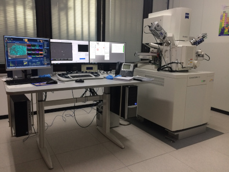
The GeminiSEM 500, purchased with the contribution of the University's "Grandi Progetti di Investimento" fund, was installed in July 2018.
The SEM with field emission source is equipped with different detectors and also provides to work in low vacuum condition mode (variable pressure) up to 500 Pa. It is equipped with EDS Microanalysis, OXFORD EDS Oxford aztec Live with Ultim Max 100 detector.
Technical characteristic
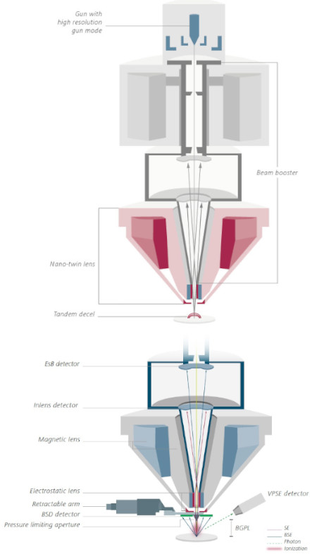
- Schottky type hot cathode field emission source
- Acceleration voltage from 0.02 to 30 KV
- Resolution: 0.6 nm at 15 KV
1 nm at 1 Kv, 0.8 nm with sample bias
1.2 nm at 0.5 Kv
- Gemini Nano-Twin lens column with beam booster and magnetic-electrostatic objective lens
- Tandem module for applying negative bias on the sample
- Variable pressure from 5 to 500 Pa. The Nano VP device reduces the beam spreading (skirt effect) typical in low vacuum conditions, in order to reach high resolutions even atlow acceleration voltages (1.3 nm at 3 KV and 30 Pa) and optimize performance in microanalysis.
- Motorized eucentric 5-axis sample stage
- Peltier cooling system for stage (-30°C to -50°C)
- Integrated plasma cleaner
- Remote controller
Softwares
- SmartSEM software with Image Navigation function for Correlative Microscopy
- 3D surface Modeling for the three-dimensional topographic reconstruction of the sample surface
Detectors
- In-Lens Detector for Secondary Electron (SE)
- In-Lens Detector EsB (Energy selective Backscatter) for high-angle backscattered electrons (BSE)
- In-Chamber Detector SE
- In-Chamber Detector BSE with four indipendent sectors and fifth additional sector for topographic images and long working distances
- VPSE Detector for SE in low vacuum conditions
- BSE Detector integrated with the Nano VP device
- aSTEM Solid State Detector with 7 annular segments for BF, DF and HAADF
- Cathodoluminescence Detector
- Sample induced current meter
- CCD IR Camera